Designing a Printed Circuit Board (PCB) enclosure is a crucial aspect of electronic product development. This comprehensive guide delves into the intricacies of PCB enclosure design, providing insights, tips, and best practices to ensure your electronic creations are not just functional but also aesthetically pleasing and robust.
Understanding the Significance of PCB Enclosure Design
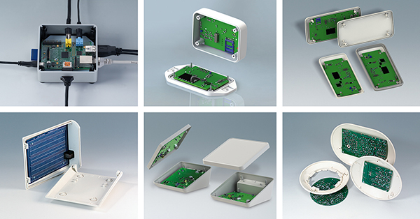
What is a PCB Enclosure?
A PCB enclosure, also known as a housing or case, is the protective covering that houses the electronic components of a PCB. It serves multiple purposes, including safeguarding components from external elements, providing structural support, and contributing to the overall aesthetics of the electronic device.
Importance of PCB Enclosure Design
- Protection from Environmental Factors: The enclosure shields the PCB and its components from environmental factors such as moisture, dust, and physical impact, ensuring the longevity and reliability of the electronic device.
- Aesthetic Appeal: A well-designed enclosure enhances the visual appeal of the electronic product, contributing to a positive user experience and marketability.
- Thermal Management: Efficient enclosure design facilitates proper heat dissipation, preventing overheating of components and ensuring optimal performance.
- User Accessibility: Consideration of user interface elements in the enclosure design is essential for user-friendly interactions with the electronic device.
Key Steps in PCB Enclosure Design
1. Define Design Requirements
Clearly outline the design requirements for the PCB enclosure. Consider factors such as the size of the PCB, the types of components housed, user interface elements, and any environmental considerations. This initial step lays the foundation for the entire design process.
2. Material Selection
Choose materials that align with the functional and aesthetic requirements of the enclosure. Factors to consider include durability, heat resistance, conductivity (if applicable), and the potential for customization or branding.
3. Enclosure Type
Select the appropriate enclosure type based on the specific needs of the electronic device. Common types include open-frame enclosures, closed enclosures, and rack-mounted enclosures, each suited to different applications.
4. Considerations for User Interface
Integrate elements for user interaction, such as buttons, displays, or ports, into the enclosure design. Ensure accessibility without compromising the overall integrity of the enclosure.
5. Thermal Considerations
Incorporate features that aid in thermal management, such as vents, heat sinks, or cooling fans. Efficient heat dissipation is critical to preventing component damage due to overheating.
6. Design for Assembly and Manufacturing (DFM)
Optimize the design for ease of assembly and manufacturing. Consider factors such as the simplicity of component placement, the feasibility of mass production, and the overall cost-effectiveness of the manufacturing process.
7. Testing Prototypes
Iterative testing of prototypes is essential to refine the design. Conduct functional tests to ensure components fit securely, thermal management is effective, and user interface elements function as intended.
Tips for Effective PCB Enclosure Design
1. Prioritize Functionality
While aesthetics are important, functionality should be the primary focus. Ensure that the enclosure design supports the optimal performance of the electronic components.
2. Embrace Modularity
Design the enclosure with modularity in mind. This allows for easier upgrades, repairs, and customization, catering to potential future iterations of the electronic device.
3. Optimize Space Utilization
Efficiently utilize the available space within the enclosure. This involves strategic component placement, cable management, and consideration of future expansion possibilities.
4. Address Electromagnetic Compatibility (EMC)
Consider electromagnetic compatibility during the design phase to minimize interference and ensure the electronic device complies with regulatory standards.
5. Pay Attention to Sealing
If the electronic device is intended for outdoor or harsh environments, proper sealing is crucial. Choose sealing methods and materials that provide adequate protection against moisture and dust.
Common Challenges in PCB Enclosure Design and Solutions
1. Space Constraints
Challenge: Limited space within the enclosure can pose challenges in accommodating all necessary components.
Solution: Prioritize components based on their criticality and explore compact, space-saving design solutions.
2. Heat Management
Challenge: Overheating can occur if thermal considerations are not adequately addressed.
Solution: Incorporate heat sinks, vents, or cooling fans into the design to ensure effective heat dissipation.
3. Aesthetic Integration
Challenge: Balancing aesthetics with functional requirements can be challenging.
Solution: Seek a design that seamlessly integrates aesthetics with the overall functionality of the electronic device.
4. Cost Considerations
Challenge: The choice of materials and manufacturing processes can impact overall costs.
Solution: Optimize the design for cost-effectiveness without compromising quality, functionality, or durability.
5. Accessibility and User Interface
Challenge: Ensuring user-friendly accessibility and an intuitive user interface can be complex.
Solution: Conduct usability testing and gather feedback to refine the design for optimal user interaction.
Case Studies: Successful PCB Enclosure Designs
Explore real-world examples of successful PCB enclosure designs, highlighting innovative solutions, and lessons learned from each project.
1. Case Study 1: Smart Home Device Enclosure
2. Case Study 2: Industrial Control Panel Design
3. Case Study 3: Wearable Technology Enclosure
Future Trends in PCB Enclosure Design
1. Sustainable Materials
As environmental consciousness grows, the use of sustainable materials in PCB enclosure design is expected to rise, contributing to eco-friendly electronic products.
2. Integration of Smart Features
The future of PCB enclosure design may see an increased integration of smart features, such as embedded sensors or connectivity options, enhancing the overall functionality of electronic devices.
3. Customization and Personalization
Consumers are increasingly seeking personalized electronic products. PCB enclosure design trends may involve customizable options, allowing users to tailor the appearance of their devices.
4. Advancements in Additive Manufacturing
The evolution of additive manufacturing, including 3D printing, is likely to influence PCB enclosure design by offering more intricate and customized designs.
Conclusion
Designing a PCB enclosure is a multifaceted process that demands careful consideration of functional, aesthetic, and manufacturing aspects. By understanding the key steps, incorporating effective tips, addressing common challenges, and staying informed about future trends, you can master the art of PCB enclosure design. Whether you are a seasoned engineer or a newcomer to electronics design, this guide equips you with the knowledge to create PCB enclosures that not only protect electronic components but also elevate the overall user experience.
Unleash innovation with MLVOLT, your premier industrial design partner. Elevate your product visions to reality with our expertise in creative design, cutting-edge technology, and collaborative excellence. Explore our portfolio and services for a transformative design journey. Visit our site today to bring your ideas to life!

Founder of MLVOLT PRIVATE LIMITED
& Ex-marketing manager of MBA CHAI WALA