In the ever-expanding landscape of the Internet of Things (IoT), the design of Printed Circuit Boards (PCBs) plays a pivotal role. This comprehensive guide explores the challenges inherent in PCB design for IoT devices and provides insightful solutions to navigate the complexities of this evolving technology.
Understanding PCB Design for IoT
Definition and Significance
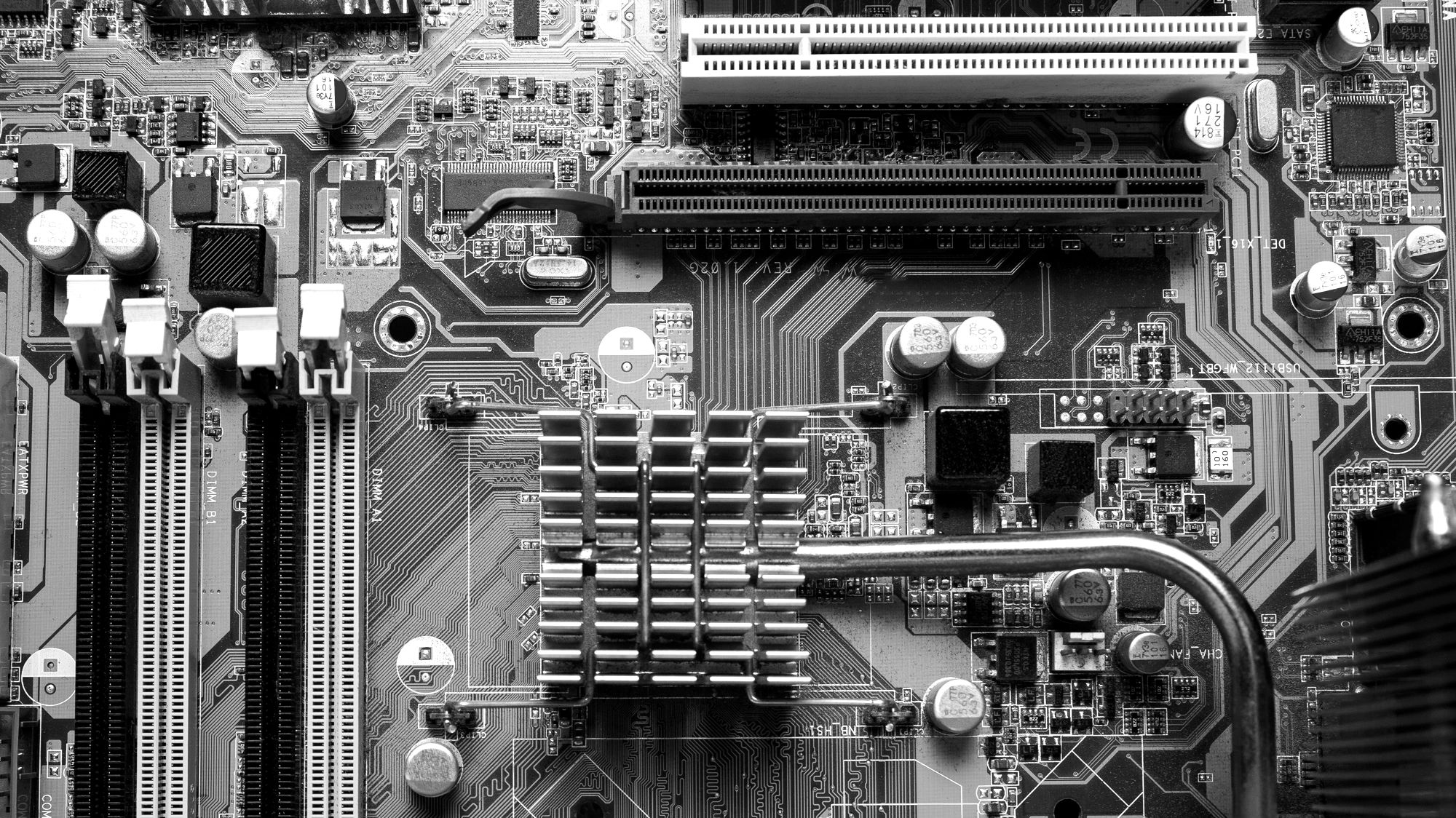
PCB design for IoT involves creating circuit boards that power and connect the myriad devices constituting the Internet of Things. The significance of robust PCB design in IoT lies in its influence on the device’s functionality, reliability, and overall performance.
Key Considerations
- Size and Form Factor: IoT devices often demand compact and efficient designs. PCBs must be tailored to fit within the limited space constraints while ensuring optimal functionality.
- Power Consumption: Energy efficiency is paramount in IoT devices, necessitating careful consideration of power consumption during the PCB design process. Low-power components and efficient layouts are crucial.
- Connectivity Requirements: IoT devices rely on seamless connectivity. The PCB design must accommodate various communication protocols, such as Wi-Fi, Bluetooth, or Zigbee, depending on the device’s intended application.
Challenges in PCB Design for IoT
Miniaturization
- Component Density: The demand for smaller IoT devices requires a higher component density on PCBs. This poses challenges in terms of routing traces and managing heat dissipation in confined spaces.
Power Integrity
- Power Distribution Networks: Maintaining power integrity is challenging, especially in IoT devices with varying power requirements. Ensuring a stable power distribution network becomes critical to avoid performance issues.
Signal Integrity
- High-Frequency Signals: IoT devices often involve high-frequency signals, making signal integrity a primary concern. Issues like signal loss and electromagnetic interference (EMI) must be carefully addressed during PCB design.
Thermal Management
- Heat Dissipation: Miniaturization and increased component density contribute to heat generation. Efficient thermal management strategies, such as heat sinks and proper component placement, are vital for preventing overheating.
Design for Manufacturing (DFM)
- Cost-Effective Production: PCB designs must align with cost-effective manufacturing processes. Considering factors like panelization, assembly efficiency, and material selection helps optimize the production cost of IoT devices.
Solutions to Overcome PCB Design Challenges
Advanced Design Tools
- Simulation and Modeling: Utilize advanced design tools that offer simulation and modeling capabilities. These tools help predict and address issues related to signal integrity, thermal management, and overall PCB performance.
Multi-Layer PCBs
- Optimal Layer Allocation: Implement multi-layer PCBs strategically to accommodate complex designs. Proper layer allocation facilitates efficient routing, reduces signal interference, and enhances thermal dissipation.
Component Placement
- Strategic Component Placement: Thoughtful placement of components is crucial for mitigating challenges associated with miniaturization and thermal management. Strategic arrangement improves signal integrity and aids in efficient heat dissipation.
Power Delivery Network (PDN) Design
- Optimized Power Distribution: Employ advanced PDN design techniques to ensure stable and efficient power distribution. This includes careful consideration of power planes, decoupling capacitors, and impedance control.
Collaboration and Prototyping
- Cross-Disciplinary Collaboration: Foster collaboration between hardware and software teams to address challenges related to connectivity and functionality. Cross-disciplinary collaboration enhances the overall design process.
IoT Device Prototyping and Testing
Rapid Prototyping
- Iterative Prototyping: Embrace iterative prototyping to test and refine PCB designs. Rapid prototyping allows for quick identification and resolution of issues before finalizing the design.
Testing and Validation
- Comprehensive Testing: Conduct thorough testing and validation throughout the design process. Functional testing, thermal testing, and signal testing are essential to ensure the reliability and performance of IoT devices.
Future Trends in PCB Design for IoT
5G Integration
- Enhanced Connectivity: The integration of 5G technology in PCB design will revolutionize IoT connectivity, enabling faster data transfer rates and supporting a more extensive range of IoT applications.
Edge Computing
- On-Device Processing: PCB designs for IoT will increasingly incorporate edge computing capabilities. This shift allows IoT devices to process data locally, reducing latency and dependence on centralized cloud servers.
AI-Driven Design
- Artificial Intelligence Integration: AI-driven design tools will become integral to PCB design for IoT. These tools leverage machine learning algorithms to optimize designs, predict performance, and streamline the development process.
Advanced Technologies in PCB Design
3D Printing Integration
- Customized Enclosures: 3D printing is increasingly integrated into PCB design to create customized enclosures for IoT devices. This allows for more compact and tailored designs, addressing both aesthetic and functional requirements.
Flexible and Rigid-Flex PCBs
- Adaptability to Form Factors: The use of flexible and rigid-flex PCBs allows for greater adaptability to various form factors. This flexibility is particularly advantageous in IoT devices where unconventional shapes and sizes are often desired.
IoT Security Considerations
- Embedded Security Features: PCB designs for IoT are incorporating embedded security features to address growing concerns about cybersecurity. Implementing secure elements and encryption protocols directly into the PCB enhances the overall security posture of IoT devices.
Sustainable PCB Materials
- Environmentally Friendly Practices: There is a growing emphasis on using sustainable and eco-friendly materials in PCB design for IoT devices. Designers are exploring materials with lower environmental impact to align with global sustainability goals.
Enhanced Power Harvesting Techniques
- Energy Harvesting Integration: PCB designs for IoT are increasingly incorporating enhanced power harvesting techniques, such as solar cells and kinetic energy harvesting. This enables IoT devices to harness ambient energy, reducing dependency on traditional power sources and enhancing sustainability.
Conclusion
Designing PCBs for IoT devices presents a unique set of challenges, but with strategic solutions and a forward-thinking approach, these challenges can be overcome. Embracing advanced design tools, optimizing component placement, and incorporating rapid prototyping and testing methodologies are key elements in ensuring the success of PCB designs for the ever-expanding realm of the Internet of Things. As IoT continues to evolve, staying abreast of emerging trends and technologies will be crucial for designers seeking to create innovative and efficient IoT devices through effective PCB design.
Elevate your projects with MLVOLT, a leading PCB design company committed to excellence. Explore our comprehensive services, blending precision and innovation. Visit our services page for tailored solutions that transform your ideas into exceptional electronic realities.

Founder of MLVOLT & Ex-Marketing Manager of MBA CHAI WALA